Semiconductors – one way, then another
Semiconductors are chemical substances that have the properties both of electrical conductors and of non-conductors – hence semiconductors. As microchips, they are built into practically every kind of electrical system. They are a key technology of the connected world.
Silicon/silicon carbide – the raw material of the connected world
Silicon (Si) is the most frequently used semiconductor in microelectronics. In chip production, ultra-pure, monocrystalline silicon is used. With silicon carbide (SiC), carbon atoms are additionally integrated into the lattice structure of silicon during the manufacturing process. This serves to increase energy efficiency.
Wafers – the semiconductor world in disc form
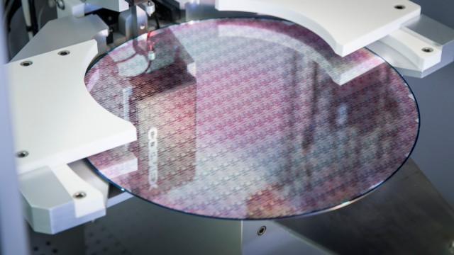
In the world of semiconductors, the term “wafer” means a circular disc made of a material such as silicon or silicon carbide. In a drawing process, cylinders of the raw material of up to 300 millimeters in diameter and more than one meter in length are extracted from a molten bath of the semiconductors. These cylinders are then sawed into discs – the so-called raw wafers. These discs are thinner than a millimeter. In a manufacturing process lasting around 14 weeks, these discs are turned into semiconductor chips.
MEMS – seeing, feeling, smelling
Rectangular or square, smaller than a pinhead, and between one and four millimeters tall – the tiny MEMS sensors are hugely versatile all-rounders in the connected world. MEMS stands for microelectromechanical systems. They act effectively as sensory organs in a wide range of different applications in vehicles and supply the control units with important information, such as whether the car is spinning on a slippery road surface. Nowadays it is also impossible to imagine consumer and entertainment electronics without MEMS sensors. For example, they transform a simple cellphone into a smartphone that takes sharp photos with no shaking or jittering. MEMS sensors consist primarily of a MEMS element and an ASIC on a tiny circuit board. The whole lot is covered by a protective casing.
ASICs – chips with built-in “intelligence”
If MEMS sensors are the sensory organs of the connected world, then application-specific integrated circuits (ASICs) are the brains. They process the information from the MEMS sensors and trigger further actions. For instance, they tell the airbags in a vehicle when exactly they should deploy. On the silicon chips measuring just a few square millimeters, there are complex circuits with up to several million individual electronic functions.
Power semiconductors – brimming with strength
These special semiconductor components look after the controlling and switching of high electrical currents and voltages. To manage this, they are equipped with special switching and conducting properties, as the high currents and voltages would destroy ordinary semiconductor components. In electric and hybrid vehicles, they control the energy flow in the power electronics between the battery and the e-motor and ensure that the electricity is used as efficiently as possible.
Clean rooms – not just clean, but squeaky clean
In the manufacturing rooms for semiconductor production, it must be ensured that there is absolutely no dust or other contaminating particles present in the ambient air. Even the tiniest of particles can destroy semiconductor components. Therefore, the air is kept clean using special extraction and filtering technology. There are various clean room classes. Sensitive chip manufacturing requires the purest Class 1. For work clothing, this means: coverall, gloves, hood, and face mask. And make-up, lipstick, and eyeliner are a no-go.


